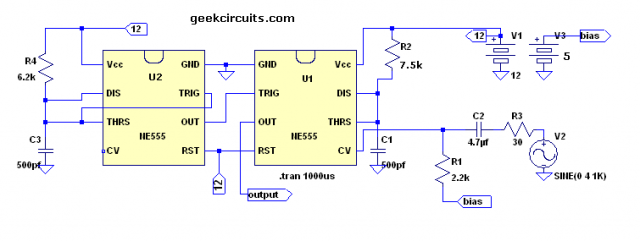
This is a continuation of my previous article regarding class d amp using 555 timer chip. Looking back to several schematics on that article, some of you may wonder why I include another 555 as U2 in the drawing. The main purpose of this U2 is to establish constant frequency trigger on pin 2 of U1 in such a way of maintaining stable PWM carrier frequency during audio input modulation.
Schematic of dual 555 circuit
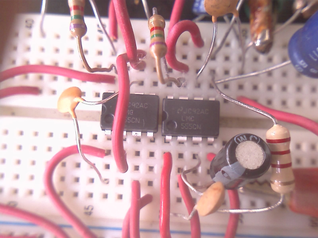
Dual 555 circuit. It is sometimes necessary to tweak the resistance of resistors slightly different from their LT spice model circuit. Oh well
By scrutinizing the behavior of the circuit in LT spice simulator, and listening to their sound thru the breadboard circuit layout, the sound is good and clean. Of course there are some interesting ways in doing this but the most interesting thing for me to satisfy my curiosity is to try to use U1 alone without the trigger U2 to conserve space and cost to the lowest value as possible. In this case, by feeding back the output pin 3 to the RC time network on pin 6 & 2 the resulting switching mode is astable with 50% duty cycle. I tried to apply music to pin 5 as usual but noticed a distorting sound even at lower volume settings.
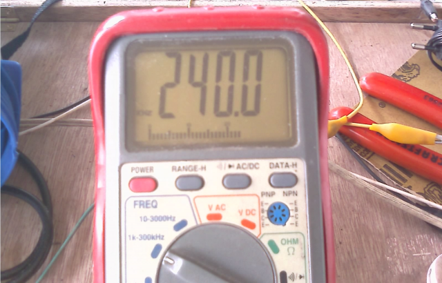
Oscillating frequency of the circuit at 240khz
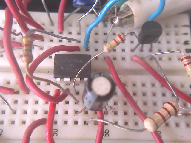
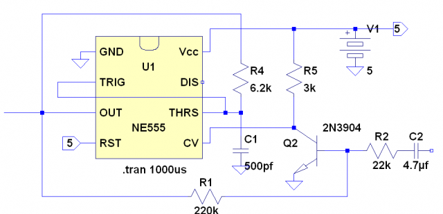
Single 555 timer with added 2N3904
Fig. 1 Schematic of 555 circuit with negative FB added. Please take note that 2N3904 varies on their hfe depending on it’s production binning. So you may get different sound quality due to this variations. Better opt for opamp if you want.
By implementing negative feedback thru the help of 2N3904 transistor to self bias it in a conventional way, (see fig. 1) the resulting sound was so good that it seems better than the sound produced by using 2 chips. Why? Well, I don’t have specific answer for this question at the moment and by observing the behavior of the waveforms while the circuit is being modulated reveals a mixture of PWM and FM at the same time. It is quite surprising for me to hear a music in class d amp having a mixture of PWM with FM owing to the fact that most of my class d design works are always time based as opposed to self oscillating approach. I think class d amp design based in self oscillating mode experience the same thing like this which makes it (self oscillating) more favored my most audiophiles. More circuits to follow.
Thanks for visiting my site

Is it possible to use the output of the 555 to drive a pair of ‘fets for higher output capability? I did toy around with the basic 555 astable circuit with audio input on pin 5 and it didn’t sound all that bad, but i got stuck after adding the FET – i got tons of DC offset on the output, and adding a capacitor in series to remove it messes up the sound.
I’m more of a class A/AB audio guy so i have to ask – will using two fets with +/- power supply (like class AB) get rid of the offset? Any calculations? I know how to calculate class A and AB amps with bipolar transistors but don’t know much about mosfets.
To avoid DC offset, you have to make sure output at pin 3 is at 50% duty cycle.That’s half of VCC on your DMM. If its not, you have to tweak the voltage at pin 5, thats collector voltage of 2N3904 and tweak R5 and R2 to accomplish this. To amplify this you have insert dead time generator before fet driver to avoid cross conduction. I’m preparing additional circuit regarding this article to avoid DC offset and cross conduction soon.
IQ spice-4
I know I´m a bit late, but how would the solution with the opamp look like? I have tried a few methods but I can´t seem to get it to work.