Class D amp using TL494 DC to DC converter chip
It’s almost 5 years now since I published a topic regarding how to use TL494 as class d amp in a popular DIY audio forum. I think it’s quite good to include this article here also. By the way, before I publish that topic I thoroughly googled the said subject to see if there are some geek guys who have already done such a playful exploit of this chip but I simply got zero hit. This could mean that I am an early bird on this regard? Or maybe I am the only one who have a bizarre taste in choosing the right chip for such an application.
I tried to check that thread three years ago and noted that the counter say 15K views as I can remember, but when I checked it out recently, it increased to more than 24K views even the thread was buried and not being resurrected. This could mean that some are still peeping on that thread and it made me to think that I am not lone odd guy after all.
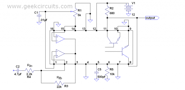
The circuit shown below is an improvised version from the original. The circuit use a NFB held at pin 3 of TL494 then feed back to pin 2 via resistor Rfb as required. The error amp output at pin 3 of the tl494 requires about 2 volts to bring the output pin 11 and 8 to 50% duty cycle. This will need a bias voltage of the same magnitude on its non-inverting i/p pin 1 as provided by voltage divider pot. The inverting input pin 2 having same level of 2 volts via Rfb completes the balance of those 3 nodes just like biasing a conventional opamp. Take note that these three pins are linear nodes and that connecting pin 3 to pin 2 in series with Rfb is a normal thing but what if we connect Rfb to the switching output of power FETs?
Figure a.
Schematic of a typical opamp biasing scheme. Pot R1 is used as DC offset null adjust and also 50% duty cycles adjust. You can connect a headphone in series with a coupling capacitor from the output to check if everything is fine.
The basic circuit above has a voltage gain of 10 based on conventional opamp gain equation of Av= R3/R4. This will require an input sensitivity of +/- 150mv to give an output of +/- 1.5 volt on pin 3 centered at 2 volts. The output at pin 11 and 8 will then modulate to approximately 5 to 95% centered at 50% on quiescent state (no audio).
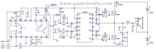
The circuit showed below implements a FB also known as “pre filter negative feedback” (NFB) and obviously far better to reduce distortion and to improve frequency response. Since this output node is a switching mode with a voltage higher than 12 volts then there must be a constant amplitude regulator before we feed the NFB to pin 2. TL494 requires single-ended supply; this makes the audio input always referenced to ground. It’s a good option to use strings of diodes to act as “amplitude chopper” in such a way of accepting only “constant amplitude PWM” signal but not amplitude modulated signal. This is an attractive option because this technique will accept only the PWM signal from the power FETs and does not require filtering before feeding back the signal to the i/p of the opamp. Another unique feature of this FB schemes is that this will make the circuit inherently immune to power supply variations without affecting the NFB voltage. This means if a fellow is using either single ended or split bus supply of 30 volts, and he decides to use 50 volts or more, as long as the drivers and tl494 supply is regulated to 12 V, and the R11 is matched with a correct wattage, then it will not affect the NFB. But if the bus supply is increased or decreased, the NFB will aggravate the output of the amplifier if it were done without those diode strings. Substituting a simple voltage divider in a form of two resistors is possible but the required voltage for FB will change if the power supply varies so diode strings is far better. For 2 volts required for feedback, the diodes strings should have 4 volts (.62V + 3.3V approx.) square wave at 50% duty cycle on idle as seen from scope. This will yield an average of 2 volts DC from your DMM. Note! Please pay attention to the “phase inversion within the loop”. This means starting from input pin 2 via Rin up to the nodes of power FETs, there should be phase inversion. Some newbie may lose their attention to this inversion when the signal is being split into two as required by FET driver. Watch closely dude.
Figure b.
There are two important things to focus your attention regarding the circuit above. These are; implementation of dead time, and make sure phase inversion is present within the loop. Disregarding these 2 things may create trouble for the newbie to achieve correct operation. Dead time network D6, D7, R6, R7 along C8 and C9 are “optional components” just in case power FETs input dead time circuit is not enough. If high idling current is present then cross conduction is at work so you know what I mean. Second thing is the phase inversion within the loop must be present. Neglecting proper pull-up and pull-down of the input pins of exclusive OR gates will jeopardize the beauty of negative feedback. You may try with no feedback at all which is done by many diyer with good result, but you have to limit the volume to avoid distortion.
Figure c.
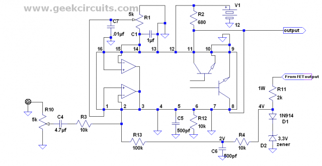
Another filtered feedback variation can be seen above. This circuit utilized RC filter with -3db roll-off at 32kHz. If you want to listen to the sound of the circuit in fig. c, you can connect directly R11 to output pin 11, 8 because phase inversion is also present within that loop (from pin 2 to pin 11, 8). Sorry for this mistake, I noticed that my 32 ohm headphone effectively “overload” the 680 ohm at pin 11 (with capacitor) giving only 0.93 volts output as measured by my DMM. I got a distorted sound due to that and this loading also create wrong bias voltage to pin 2 as well. So, listening to this output with NFB and headphone together is not advisable.
Take note that removing RC filter R4 and C6 and connecting R11 directly to output pin 11,8 will produce good sound quality as well (yes, this is true if headphone is not connected there) possibly if additional buffer is available. Take note that small amount of DC offset is still present from the output and this is a function of parameter spread variations such as diodes voltage drop per degree C, supply voltage changes and etc. Simply adjust the pot at pin 14 to reduce the offset to the lowest as possible. I always favor a pot to null the DC offset or adjusting to required 50% duty cycle.
Designing a class D from scratch is a tough proposition especially for a beginner. This might put Tl494 in the prime list of a newbie’s baby step towards such first attempt. The availability and low cost nature of this chip coupled with high degree of repeatability, simplicity and stable in operation will surely improve the skill of a beginner. If he is creative or little bit ambitious enough; with guts so to speak, he will be surprised to see how practical tl494 to be use as a class D audio source. The very first Tl494 that I experimented was just extracted from a junk ATX power supply but when I put it on the breadboard with some caps and resistors the sound is surprisingly good!
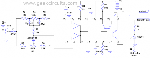
Case in point: Tl494 contains three independent i/p pins that can be tailored to suite your listening needs. In my prototype an active band pass filter is tuned to 20 Hz (I love 20 Hz bass), another one as full audio band and then pin 4 take care of the treble at 7kHz, (I like rich in treble also). This practical approach simply eliminates my needs to build additional active crossover network. It’s totally complete inside the chip.
Figure d.
Suggested circuit employing tuned band pass active filter using the lower opamp as “mega bass enhancer” that peaks at 20Hz with +/-7Hz bandwidth. Then upper opamp is a simple full audio band, while pin 4 takes care of the treble with -3db roll-off at 7 KHz.
Did you notice the additional pot R9 from the circuit above? This is another adjustment for removing the offset voltage from the output because pin 4 requires 1.65V bias voltage as compared to pin 2 that needs 2V.
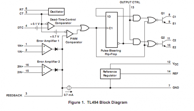
Let’s explore the innards of Tl494. Data sheet says; if the voltage at dead time pin 4 is varied from 0 to 3.3 volts, the output duty cycle will change from 3% to 100% (that’s non-inverting relative to output pin). Also, if the voltage is varied from .5 to 3.5 volts at pin 3, the duty cycle will vary from 97% to 0% (that’s inverting relative to output pin). By the way, this pin 3 voltage should be centered at an average of 2 volts (.5+3.5/2) and also to pin 4 (0+3.3/2= 1.65V) to get 50% duty cycle from the output. Also take note that the author of the PDF did not mention if the output transistors are configured as emitter follower or just common emitter. These statements on PDF may confuse some folks (mind you, me too 6 years ago) but I just simply think that the author’s assumption referred it as common emitter which is just fitted to the statement above. I also verified that on breadboard long time ago and it’s correct. The schematic in Fig. b shows that the 2 output transistors are configured as common emitter.
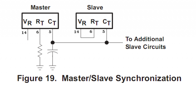
Synching of tl494 for multiple channel application.
Synchronizing multiple channels using tl494 is easy without any problem regarding audible bit frequency to occur compared to self oscillating class D approach.
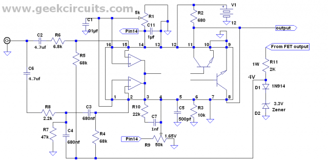
Here is another suggested circuit employing the popular “bass and treble” tone control being used from linear circuits that most of you are familiar with.
Figure e.
The circuit above requires +/- 1.5 volt of input to get the required +/- 1.5 volt output from pin 3. This is due to the nature of this tone control network. When the 2 pots are both at their midpoint position then the voltage gain is 1 at pin 3.
Before you try any of the circuit shown above, try it first on the breadboard so that you can tweak the bass, the mids and high frequency by altering the R or C to your desired audio band. Or you can simply use only one opamp with one fb resistor to be simple one.

Many thanks for explaining this circuit once again, between the ones who were reading that thread on DIYAudio there was myself as well. I’ll be building this class D amplifier with TL494 in the next couple weeks, so if you have any other things to say that would help me in my endeavor, please do.
I will be using IR2113 as driver, the output transistors are not decided yet. I’ll probably use transistors from a motherboard for the prototype, then move on to higher voltage ones once i’m accustomed to the circuit. My final target is 250W @ 8ohm, this is to be a subwoofer amp (and yes my sub driver happens to be 8 ohm).
By the way i’m slowly learning more things about my little 555-based supply, and i’m ironing out its quirks one by one. I’m a bit put off by the behaviour of pin 7 though, ultimately using pin 7 is the reason why my waveform isn’t too square. But it’s sooooo clean… Oh well. I’ll first install a proper comparator into that circuit, then i can worry about everything else.
Your initial target of 250W looks great but make sure all things must be tried first in breadboard. Every time I perform any circuit design, I always use breadboard and its so easy to tweak anything there like bass and treble tweaking. No, I didn’t mean you will use breadboard at that power level but something less than 3W at 12V is just fine. If you are satisfied how it sound in breadboard, then you can finalized to PCB.
Eh, i don’t use breadboard, i use stripboard and point-to-point wiring. Sturdier and cheaper IMO. I won’t need any controls except lowpass and highpass filters to protect from over-excursion and those will be built separate from the TL494 anyway. It might need a volume knob tho… Come to think of it, i’m so used of turning the volume knob on my amp that having another one will be a bit of a shock.
I will be passing both the sub and the mains thru my 10-band EQ then separate the signal with active filters. The lower three bands are at 31, 63 and 125Hz which should be enough control.
hi
i want make switching supply . iselect tl494 and disign it. but for control section , icant understand that how can find gain of this chip ,when pin3 of it have 0.7 v or lower pwm is 0.45 – 0.50 but when pin3 have 2.5-4.5 v pwm is 0.
i want it for control current circuit.
can help me?
Please try to download this pdf from TI because most of the answers from your questions can be found there.
You can also try to re-read my post carefully because I already mentioned about the specific voltage from pin 3 to get the desired PWM output from pin 11, and 8. By the way don’t forget to dis-able the 2 opamps if you want to use pin 3 as the control pin for PWM regulation on the output.
Cheers
Hi
I am very much interested in building this circuit. I haven’t worked with electronic components in a long time. I just couldn’t help but notice something that might look like an error in your circuit. Maybe it’s just a symbol I am failing to understand. Normally a speaker would connect to GND like you did, but now why is the VSS also symbolled the same way? I would like to assume the TL 494 connects to GND like the load. I would also like to think the driver does not share the same GND plane, therefore what seems like GND there actually connects to -VCC, except for pins 2 and 11. Please help me get this out of the way.
Class d amps are powered by either single or split supply. In half bridge topology, Conventional class d amp circuits utilizing opamps are usually powered by split supplies. This means the input signal and the load speaker is always referenced to neutral ground (+VDD, -VSS with neutral ground). My circuit utilized combination of both single and split supply. This means tl494, along with Exor gates and the FET driver requires separate single +12VDC with its negative connected to –VSS which I referred to as the ground. The load speaker is then connected to center tap of the supply AKA “neutral”. Of course this speaker neutral node is not necessary if you use full bridge topology. Unfortunately, my circuit is just a simple half bridge. I hope it helps.
Cheers
Many more thanhs regarding classd power amp and preamp design Mr Geek.folllowing ur concept here we design 3000w high power PA amp system with smps &test has been taken to comercialization of this amp .thanks for ur ideas.
Please take note that this class D audio amp circuit was intended for newbie or students alike looking for a practical audio circuit to play and to learn with. Of course it is free and open to anybody without copyright issue. But please bear in mind that this is not “hi fi” and TI says these chips are for smps applications only. It just so happen that most DC to DC converter chips can play music if you are creative.
Thanks for dropping by
cheers
I need a circuit converter 12VDC to 340VDC , it use TL494 , mosfet and Transformer.who can help me ?Thank for all !
What do you think about it:
http://www.diyaudio.com/forums/class-d/178968-class-h-amplifier-idea.html
Hi friend!!! thank you very much for your work and explanations. I just builded a full-bridge amp based on your topology. I use 2xIR2110 driving four IRFB4227 MOSFETS, I have changed dead time /discrimination circuit by ultra fast NAND gates and its sounds pretty good for this old frecuency limited PWM chip (TL494). The best goal of my configuration is that now possible to feed the entire amp from 12V, now I’m working on buck switching regulator to elevate from 12V to 80V and use this amp for a car. Regards!!!
nice….circuit for new ideas….
Hi,Would you put up the LTSpice files for simulating this please ?
sorry, LTspice doesn’t have TL494 model available in their library. I just tested it via breadboard.
Thanks for dropping by
Hello there, just became aware of your blog through Google, and found that it is truly informative. I am gonna watch out for brussels. I will be grateful if you continue this in future. Lots of people will be benefited from your writing. Cheers!
I greet you here on the server, just by chance I found the idea – TL494 in the function driver for D-class amplifier, which I have dealt with the 12 to 15 years, and based on this circuit and the drivers from IR (everything was then at the Czechoslovakia more … poorly accessible, and good Feta). At that time I developed and produced a pretty good power amplifier with this line-up for the band. We have few people even knew what the D-class amplifier, and I offered a power of 2 x aplifiers 800-1200W/8-16Ohm weighing 4 kg! Bomb! Amps were without transformer, pulse stabilizer directly from 220V, and then straight “Pulse Audio Converter” and output to the speakers via the speaker demanding filtry.Outputs are electrically connected to the network 220, but it’s too much not iterested.Also walked on the heights (from about 8 kHz), but it did not matter, it is important for big-beat bass. It was probably because they were not so quick and good quality feta, and had to be longer and lower sample Deadtimy frekvency.Ale just great! Second driver from IR and 494 I think there were only two operating amplifiers in the feedback for frequency filtering and suppression of DC offset, the 494 was good transistor amplifier with feedback controlled servo feedback from operampli.Bigests and heaviest components of the output filters, much depended on the characteristics of properties in the large condenser power.A half-bridge to 400V, as Feta half-bridge worked in half-bridge against capacitive divider good anti-puncture speakers in fetuses. Then I dealt with then ….. Ciao Sinnnaka, Prague.
can u tell me for what values i need the inductor and the capacitor at the output,.
Hello Mr. IQspice. I’ am building the amplifier from the figure b and I need some help.
I need it to work at 100W but don’t know how to calculate the values of the inductor (L1) and the capacitor (C4). I know they are there to match the speaker’s impedance but don’t know what to do. what speaker would be the best for this scenario?
Hello again Mr. IQspice:
Now I know a few things about impedance, I can handle that part but. Thanks anyway
But, I want something else, I need to simulate this circuit to see it working before build it, the problem is the spice models for the IR2010 or the TL494 are very hard to find.
Do you know where can i find them?! thanks for your work!
Hello! I am a student of electrical engineering at ITT-Tech and have a project to build an amp circuit I like the idea of working with class d technology. I am intrigued by your design. My problem is I’m working with multisim 11.0 and it does not have a TL494 or IR2010 to work with. Are there any compatible chips that I may be able to use in place of these? I thought to try to build these IC’s from scratch but find this daunting. Any suggestions?
I have to leave a comment: you’re a freaking genious! 🙂
When I was building a great self oscilating, split supply class D power amp, I learned about those amps and inmediately thought on TL494 as modulator. However, this line of thought was discarded by people I asked saying that could work, but will distort a lot to be unusable. Now, just for fun, I tried this but with a single supply, full bridge and I get impressed by the fact that something this easy can lead to outstanding results, given the fact that is not intended for this. Plus I learned new concepts and solutions from your schematics. Now I see the same but using a 555! I have to try that. Just want to say thanks!
Thank you! Barely find what you need.
i want make convertor dc to dc.i want that input 12 and out put 24/32 difrent. but i have not this circut.did u can me.
Excvelente circuito, muy creativo y me ha dado ideas de como usar este chip de la forma correcta para otros proyectos
buenas como en mi pais no se consigue el r2110 he desidido usar los driver transistorizados me fue muy bien y suena de maravilla
Hi,
nice ideas !!
Had some ideas (years ago) by Triode tubes ( 6AS7) behind this pwm chip, and was working great, with Les distortion, i remember.
But… Is there a opportunity to have an adjustable neg. peak limiter in the audio input section?
Like to use it as a presage microphone amp for my AM modulated transmitter in the amateur bands.
Greetings,
Hans.
Why didn’t you use internal dead time circuitry of the TL494? Why are two output collectors connected with each other? Wouldn’t it be better to connect each collector to separate resistor and use it to complementary drive HIN and LIN? This would make the use of XOR gates unnecessary.