It’s more than one month now since I updated my last post and I regret that I couldn’t post anything within that length of time. This is due to the nature of my job. We left Tilbury last month and now we transferred here in Bremerhaven shipyard and our ship is still being dry docked for repair. Unfortunately we still don’t have any internet connection and our satellite is still under repair too. I just rely on outside wifi access so, this is my new follow up post as continuation for the unfinished topic for that post below. Hopefully, I will make a new post again if our internet connection will be restored soon.
My last article was still 555 timer so this is another neat idea how to get more useful circuit out of your 555 timer. I think it is not good to move on to another topic using another chip because every time I made a circuit out of this 555 timer, another idea pops-up in my mind to share.
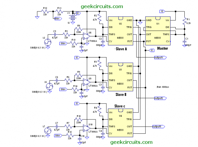
OK, here we go. Lets say a fellow wants to build a 2 channel class d amp using 555 timer. This is a bit tricky because using 2 of this chips will oscillate in different manner even if the frequency determining networks are ideally matched. So the need for syncing is a must. Quick thinkers immediately had in mind is that the circuit should have a master and a slave part for proper syncing of carrier signal to avoid audible bit frequency. Yes, this approach is correct but how to implement it? So here is a possible circuit that may pop-up in the mind of quick thinkers.
The circuit shown above was copied from my previous circuit I discussed recently. Here, pin 6 and 2 of slave A and B is being connected to the master pin 6 and 2 for syncing. The master controls the frequency of oscillation. This is the easiest and maybe the simplest syncing scheme that you may think (mind you, me too). But upon simulation, when the audio signal is introduced to either slave A or B, the output pulses to pin 3 does not behave as expected. Even if I carefully tuned pin 5 to any offset voltage that could bring the output more usable seems difficult.

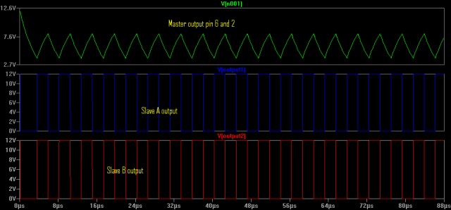
The output waveform of either slave A or B looks promising if no signal is present on pin 5 (pin 5 is floating).
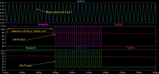
But when audio signal is present, and the collector of 2N3904 is connected to pin 5,my enthusiasm to the circuit suddenly collapsed.
Output waveform of pin 3 in both slave A and B. Here, the output pulses are intermittently put into a halt by the Vmax and Vmin of 1 kHz audio input. I think that there is no simple remedy available here for the moment.
This made me to conclude that this type of circuit is only applicable as single channel amplifier. Careful scrutiny within the entire circuit followed by several simulations attempt leads me to think that it is only necessary to link pin 6 and 2 to its very own oscillation or modulation and should not rely to external one. There must be another way to implement two or more channel and the simple answer was already discussed by me at the very first article I post.
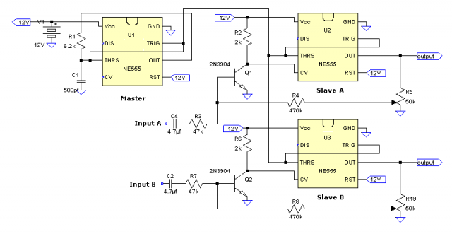
The circuit shown below will work in multiple channel application because the master’s output pin 3 has negligible loading effect of the trigger pin 2 of any slaves connected to it. Also, this circuit is quite unique in its own right because the operating principle does not conform to a conventional setting where saw tooth is generated to sample the audio signal thru comparator’s two inputs to produce PWM. Here, the master generates continuous but fixed pulse width of approximately 98% for the purpose of two important things; To reset the internal flip flop of all slaves, and to discharge the timing capacitor via pin7 simultaneously. The most attractive feature of this circuit is that they are darn cheap. This circuit can produce wider modulation from 0% to 95%. But 100% is not allowed because the master is required to pull down pin 2 to ground of all slaves in short duration fast enough to accomplish its two task as already mentioned above. Opamp bias network R11 and R12 should be replaced with potentiometer for 50% duty cycle adjust.


The master produce an output of very short negative going pulse which is sufficient to change the output state of all slaves into logic 1 but the “width” of that “on” state is governed by modulation voltage on pin 5 of all slaves.
Please take note that even though the circuit looks good and simple, proper matching of the master and slave’s frequency is very important. Improper matching will result into unsuitable for class d application. This mismatched frequency scenario I’m referring to is; instead of producing class d amp, you will end up to get a frequency divider instead. Try to simulate it so that you know what I mean.
Let’s scrutinize the basic function of the circuit. The master is wired as an astable multivibrator having a fixed frequency F determined by;

The slave which is configured as monostable or “one-shot” having a variable pulse width (PW) which is a function of;
PW= 1.1 R1 x C1
Take note That there are three possible ways in modulating the width of the pulse of the slaves; Its either to vary the timing resistor R1 or to vary the capacitance of C1, but the most easiest way is to modulate pin 5 with a correct signal. Some newbie might wonder how does PWM is being generated by simply modulating pin 5? Yeah, It is more easier to grasp the theory behind PWM generation by altering either R1 or C1, but how about pin 5? The answer is simply based on the fact that if the 3 internal voltage divider of 555 timer varies its voltage via pin 5, the cut-off and cut-in of upper and lower comparator voltages will “set” and “reset” the internal flip flop of all slaves accordingly thereby producing PWM from their outputs.
In my breadboard, R2 doesn’t exist and I can produce 97% duty cycle for use as master. If you cannot produce this without R2, then you can add R2, then follow the astable equation above. By the way, my 555 timers are all CMOS type marked as LMC 555 and they are capable of oscillating up to 3 Mhz at 5 volts. They consumed less in power but with very fast rise and fall times of 15 nanoseconds. Of course any bipolar 555 timers will work as well. It just so happen that LMC 555 is the only available stuff in my cookie jar.
Simulation of the circuit above is available below:
[smartcounter:10]


Why, ain’t that the classic 555 PWM. Fixed frequency astable with duty cycle as high as possible feeding a monostable.
I wanted to use a circuit like that for dimming some halogen spots i found for like $2, but i never got around to building mounts for the spots so i didn’t build the circuit.
However i DO have seven SMD 555s lying around doing nothing, and some PCB to spare. And a bunch of 2N3904s i intended to use as output stage for a small FM amplifier, which i won’t build anymore because i blew my modulator. Oh and there’s those 18A mosfets i recovered from that old monitor, and the TL072s i found yesterday in a drawer.
Now i know what i’ll be building. 🙂
If you intend to use 555 timer as dimmer for halogen or high power LEDs then a single 555 timer wired as astable shown here will suffice. The output of the two complementary pair transistors can drive high current mosfet of your choice. The pot can be varied from 0 to 100%.
Thanks for the dimmer circuit, i’ll try it out sometime. I have recently acquired a ‘scope so 555 class D is one step closer.
Right now i was probing around in a 555 boost converter that i never got to work properly, load voltage would drop like crazy and the mosfet got quite hot. I found HUGE amounts of ringing – and at 48MHz!!! I didn’t know i built a radio jammer instead of a power supply… I’ll be experimenting with snubbers and see if i can get things to work better. Having a scope certainly is great help.
You might wanna look at this circuit: http://www.dprg.org/tutorials/2005-11a/index.html
It’s a rather clever way of getting “true” PWM output from a single 555. I haven’t experimented with modulating it with an actual signal yet, but i will do. But one of the things i like best about it is that the discharge pin does not exhibit the ringing of the output pin, it should be better suited for simple switchmode or audio apps.
I have designed and simulated a 3.7v -> 12v boost converter inspired from this circuit. In my case i use PSM (pulse skipping modulation) ie a comparator drives the RST pin low when voltage reaches the desired value. As opposed to pin 3 it requires external driver transistors, but the pulses are a lot cleaner, and simulated efficiency is 90 to 94% from 300mW to 1.3W output. The disadvantage is rather large spikes of ~700mV with 100uF output cap, but things such as power LEDs or batteries (a solar charger maybe?) should be able to tolerate that. The circuit’s own consumption is roughly 10mW, but it can be lowered, and it’ll probably be lower in real life anyway since i will be using SMD parts.
I’ll be building it next week and telling you how it goes. I’ll also post a schematic of my circuit if you’re interested.
The drawing from that link and my dimmer circuit look and function basically the same. I have already mentioned to my previous post that the output pin 3 can be substituted with pin 7 using pull-up resistor to avoid ripple noise if required. I just add 2 complementary pair transistors in case it will drive higher capacitive load such as high power FETs in which pull-up resistor on pin 7 cannot drive gate capacitance above 5000pf. Thanks for the link by the way.
Heh, blame me for not paying attention. Anyway i’ll be building several variations of that circuit next week and see whether it gets any close to the efficiencies in the sim.
I built the circuit today and it doesn’t work as expected. The output is a sawtooth type of thing rather than a square wave, with or without driver transistors, so the drive to the FET is far from optimal. Also, twisting the pot still changes the frequency like in the regular astable configuration.
This is weird. I’ll give it a more in-depth look tomorrow.
Well i found my answer sooner than expected. I lowered the frequency in the audible range and bam, nice fat squarewave. It seems like those SMD 555s i bought aren’t any good at high frequency. And i made the board to fit them… Tomorrow, dead bug style wiring. 😛
It can’t be a measurement error because i have a DIP 555 which runs at 70ish kHz and the scope shows a square wave on that one. I’ll try that one in my circuit and see what it does.
Well, thats nice. I try to analyze the drawing maybe my schemo is not correct but it’s correct..Congrats!
Maybe the circuit i posted is wrong, as i built that one. Anyway i don’t care that much about duty cycle since i’m using pulse skipping.
I managed to get a decent waveform at some 30ish kHz out of the SMD timer. I wanted to use higher freq but oh well. But i had to learn the hard way that the 555 doesn’t reach ground anymore at high duty cycle. The DC bias built up on the MOSFET gate, and that familiar smell of fried silicon went up in the air. Oh well.
I dropped a new FET in, lowered the duty cycle some, and things are looking good. I’ll be playing with the pullup resistor on the driver transistor bases but right now it’s all looking good.
I’m testing this with a computer power supply and preliminary numbers say: 4 watts in at 5.13 volts, 3.57 watts out at 12.74 volts (have to tweak the voltage divider that drives the comparator, the voltage is slightly high). That gives 89.2% efficiency. I’ve tested it on a bunch of power resistors totalling 7 ohms, and consumption clocks in at 25W @ 5v with 20W output @ 12.03v. 82% efficiency at this load, operating in continuous mode already, the mosfet does get hot but considering it’s only got a bit of copper plane for a heatsink it does well. Not too shabby eh? The switching waveforms are nice and clean. Ripple could be better, with 100mV spikes at idle, 300mV with the 3.57W load (a 120mm computer fan), and 600mV on the 20W load. But i’m only using a single 470uF capacitor for filtering, not even a low ESR one. It gets kinda hot too btw.
The circuit uses about 11mA at 5.20v when idle, that gives about 50mW own consumption. I’m not using a Schottky diode for the output rectifier so i expect this to further improve when i will. Given that i initially wanted this circuit to run from a battery and deliver 1.3W at most, i’m quite happy with it. Next step is to make it smaller, as the T106-26 toroid i found in my junk box is a bit big compared to the other parts.
I’ll post the schematic and some pics maybe in a few hours.
The SMD timer was acting up, so i thought it would be a good idea to drop the DIP one in at this point. I am now switching at ~71kHz. The waveform isn’t “very square” but it’ll do.
The circuit exhibits some interesting behaviour – as i increase the duty cycle past the optimal value for that particular load (if i keep increasing duty cycle after the circuit enters pulse skipping mode), power consumption of the circuit goes up, although output voltage does not change. This is weird – the duty cycle pot should do nothing but set the maximum duty cycle allowed and thus define the current limit and minimum efficiency. Pulse skipping is supposed to turn the modulator OFF and “chop” whatever waveform it might be putting out regardless of its duty cycle, but it seems like that doesn’t happen. Maybe the opamp is too slow? It doesn’t make much sense to me.
Sorry for the delay, here’s some pics. http://img42.imageshack.us/g/finalschematic.jpg/
The schematic represents the actual values of the parts and the way the pot is set up, not necessarily what i used in simulation. Actually, if you simulate that, LTSpice shows that it’ll never actually reach 12 volts!
MOSFET came from a motherboard, LM324 came from another motherboard. Sure it’s a waste of a quad opamp, but it was free and it fit the requirements so why not use it. Inductors and TL431 came from a fried ATX power supply. The boost inductor (should be) 100uH, it’s 33 turns on T106-26 core. I’m sure i’ll be able to use a smaller core… I left the wire slack because i might need the whole piece of wire in some other project so why cut it. Rectifier (FUF5404), output caps and driver transistors came from a monitor. Oh and as you can see my PCB marker sucks, and my nice fat ground plane has not-so-nice little holes in it.
If it’s one thing that building this taught me, it’s – time to move on to proper PWM controllers. The UC3842 and TL494 are ridiculously cheap, and actually i have one of each in my junk box. 😛
Heh, i wasn’t about to leave this thing unfinished. I was right about the LM324 being too slow as a comparator. I bought some LM311s today.
With the 311 in the circuit things work a lot better. Pulse skipping works fine regardless of load, regulation is good, efficiency is good too. I can now twist on that duty cycle pot all day long and the output voltage won’t change unless i set it way too low. Oh and i also bought a 5k trimmer instead of that ridiculously huge pot. 🙂
So far so good, now time to make it SMALLER.
It turns out that my rounded waves were due to the capacitive loading of the 1x probe, i had forgotten all about that. I now use the 10x for all my measurements and actually the square waves were nice and crisp.
And you won’t believe what i’ve been up to – i’ve implemented my 555 skipmode controller in a 2-transistor forward smps running off the mains! And… it works. I drive a motherboard mosfet with the 555, which in turn drives a pulse transformer scavenged from an AT PSU to isolate the controller from the switches. The output voltage is sent straight to the divider which goes into the comparator, no opto since the controller and secondary are fine on the same ground, i feed the controller from a separate tiny mains transformer i had lying around.
The final target is +/-70 volts at 400W for my 8 ohm subwoofer amp. I have tested it up to 80W only as i don’t have a higher dummy load atm, but right now it is running with a 50 watt load, switching transistors on an ATX PSU heatsink WITHOUT A FAN, and the heatsink is at room temp!!! That’s some nice efficiency there. The power switches are IRF840s btw.
All it needs is a dual comparator to implement undervoltage protection, which should double as short circuit protection as well. With 1 microsecond response time, i strongly believe that it will. That’s why i decided to pursue the pulse skipping approach – no error amp so no compensation to worry about, no minimum load requirement, and damn fast response times. The only side effects are more output capacitance required, and a little hissing from the transformer. But a bit of varnish should take care of the hissing part. Right now i still have the second 70v secondary to wind (plus whatever auxiliary supplies), so the transformer hasn’t been varnished yet, but even so it is fairly quiet.
It’s been a really long way till i got here, i learned so much by reading docs and using my scope. But… i made it. 🙂 Next up, the class D amp using TL494.
Hello, i am a dawson college student from montreal. Im wondering if your schematic works with 3 channels? I plan on cascading another 555 timer and synch with your astable oscillator (master 555 timer). Do you know if its possible to “sum” them all up so i can transmit through AM or FM signal and then decode it after like radio controller cars? I plan on controlling 2 servos and 1 switch.
You can contact me by email if you want to help me out. I can pay for your time by paypal …. Thanks !!
Hi Th3_uN1Qu3,
Please send me the schematic of that ClassA amplifier which was built by your shelf.
I want to try a simple class D to get experiance.
Many thanks.