
Finally! I`m back from long hiatus!
As the subject title implies, yes. LM319 is not a popular choice as integrator/differentiator combo due to it`s output pull-up resistor which is not good to directly drive capacitive load. Although it was being claimed by chip makers as fast comparator, they mean it’s fast enough as digital pulse generator for driving TTL/DTL logic gates. This means it can generate decent PWM pulses intended for class d amp purposes but at different, or should I called it harsh method as shown in schematic diagram of Fig. 1 below.
Fig. 1 Single comparator U2 as triangular wave generator then U1 as amplifying PWM generator that can be driven by small signal audio source.
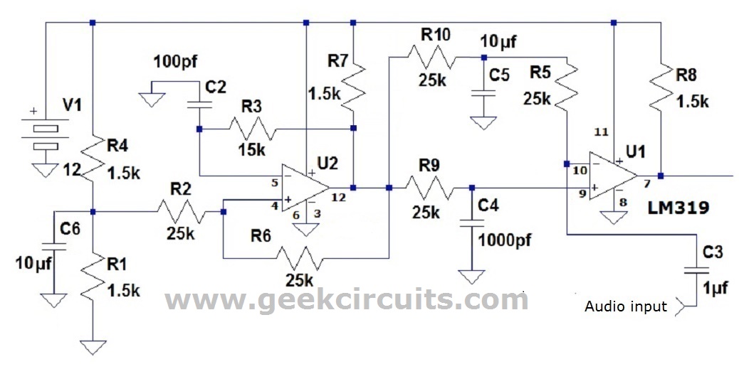
Fig. 1 Shows LM319’s U2 is wired as square wave generator whose frequency determining network is governed by R3 and C2. Then the output was terminated with R9 and C4 that serve as a triangular wave generator. Don’t laugh! I’m not done yet!.
Most experienced class d amp circuit designers are blessed with an eagle eye and can quickly spot the questionable design approach I made above (only 2 seconds is enough mind you). Yes, these dudes are understandable because what the hell am I intend to use for that kind of circuit? It’s not so linear triangular waveform as a reference in the first place! Well hold on fellas, I will show you that with a little tweaking on their timing network, then maybe this design approach may tickle your fancy in considering it. So lets dig a little bit further and fasten your seat belts.
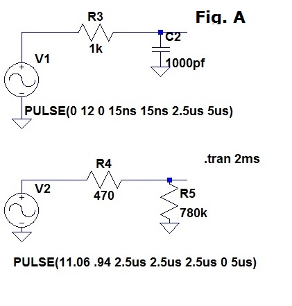
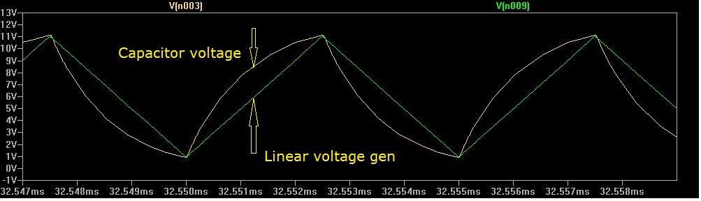
First of all, I provide a simulation in LTspice to show you the behavior of the circuit depicted in the following order. In Fig. A Capacitor C2 is being charged and discharged via resistor R3 produced by square wave source. In fig. A also (below circuit) I put a linear triangular wave generator so that you can see the two overlaid signals for precise comparison. It is forbidden for us to use this kind of bended triangular wave as a reference. The reason why it is so bent is that the capacitor is a hungry beast in the circuit – It sucked all the resources available from the source generator but the resistor cannot cope for that amount of energy (nonlinear current results). That’s why it bends a lot. If the resistor can only provide bidirectional constant current to charge and discharge the capacitor then it would be linear. But adding constant current to do that will require two faster and pricier comparators that will add cost and difficulties for beginners to tackle with. In my first circuit above of Fig. 1, only one comparator U2 is needed as square wave generator followed by U1 as an amplifying PWM that can be directly driven by any audio source. Input sensitivity will be +/- 240 mv then the output will swing from near 0 to almost VCC at 235Khz sufficient enough to drive FET drivers.
Fig. A simulation shown below with lower resistance for R3 giving higher charge/discharge current.
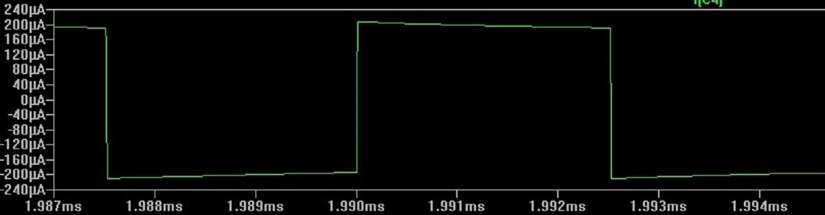
 Waveform of Fig. A showing severe bending of voltage due to nonlinear current demand of capacitor. Peak to peak current is shown bellow.
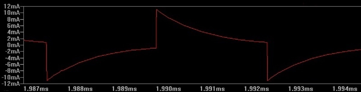
Peak to peak current of 11ma gives bended rise and fall signal.
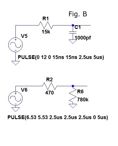
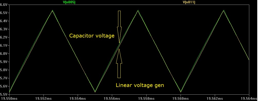
In Fig. B circuit I increased the resistance from 1k to 15k and it improves a lot giving small vertical voltage difference of 19mv compared to circuit A with 2.68 volts! The waveform is shown below.
Reducing the charging current further thru the resistor by doubling the resistance from 15k to 30k make it very near linear (yeah almost linear, lol). As you can see from the sim in Fig. C,
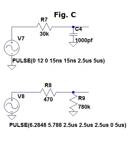 Fig. C, Overlaid Capacitor voltage and linear ramp generator are look alike now.
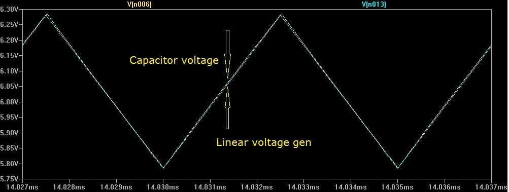
Circuit sim showing reduced charging current using 30K resistor. Then overlaid with linear signal. Now you cannot see the bended one because they are almost identical in linearity. Zooming-in is the only possible way to close examine the vertical voltage difference of the two
There is small amount of voltage difference plotted along vertical axis as small as 4.2 mv which is too small and might be considered benign. See Fig. C.
Peak to peak charging current decreased to 200ua.
This means lesser charging current means lesser voltage needed to charge and discharge giving more flatter ramping output voltage. This will also give smaller peak to peak output as the result. In this demo, R7, C4 output node yields +/- 240mv of ripple voltage (triangular wave) riding on ~6 volts DC. See fig. C with overlaid linear signal combined.
Some of you may think that 240 millivolts of triangular wave is too small for LM319 to amplify? Rest assured fellas, most comparators are designed to amplify differential voltages smaller than 5 millivolts of overdrive. So, 240mv of this sort is way too easy for LM319.
Now we are done! Biasing the comparator using this reference is the next easiest thing to do.
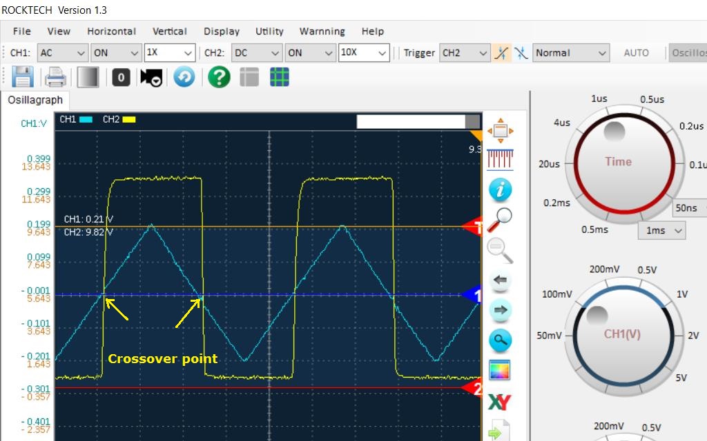
Let`s analyze the drawing of Fig. 1. Notice the DC bias resistor R10 connected to output pin 12 of U2? This node produce more than 11 volts of continues pulses at 50% duty factor, but I simply tap R10 on that output node because this is the best possible source of DC bias to pin 10 of U1 – meaning it will always seat at the crossover voltage of the triangular wave appearing on pin 9 to obtain the required 50% duty factor. Another possible DC bias to pin 10 is to use trimmer pot connected to VCC and ground then the center wiper goes to R10 but adjusting it to half of VCC to sample the crossover point of that triangular wave appearing on pin 9 would be very tricky to achieve. It works ok in sim, and also in real world (sort of) but when switched off for a while (coffee brake) and then on again, it needs recalibration again ouch!. Temperature drift and VCC fluctuation affect that trimpot DC bias. With the circuit I made above, node B always follows the crossover point of node A at all cost – it is immune to parametric changes mentioned above.
Fig. D shows simulation of what’s going on at the output of pin 12 of U2.
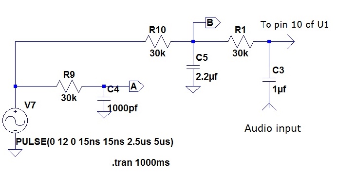

Fig. E. Output waveform at node A and B.
Thats It! time for the real world test! The picture below shows breadboard with some parts added. LM319 on the left versus Tl494 on the right for some wave form comparison.
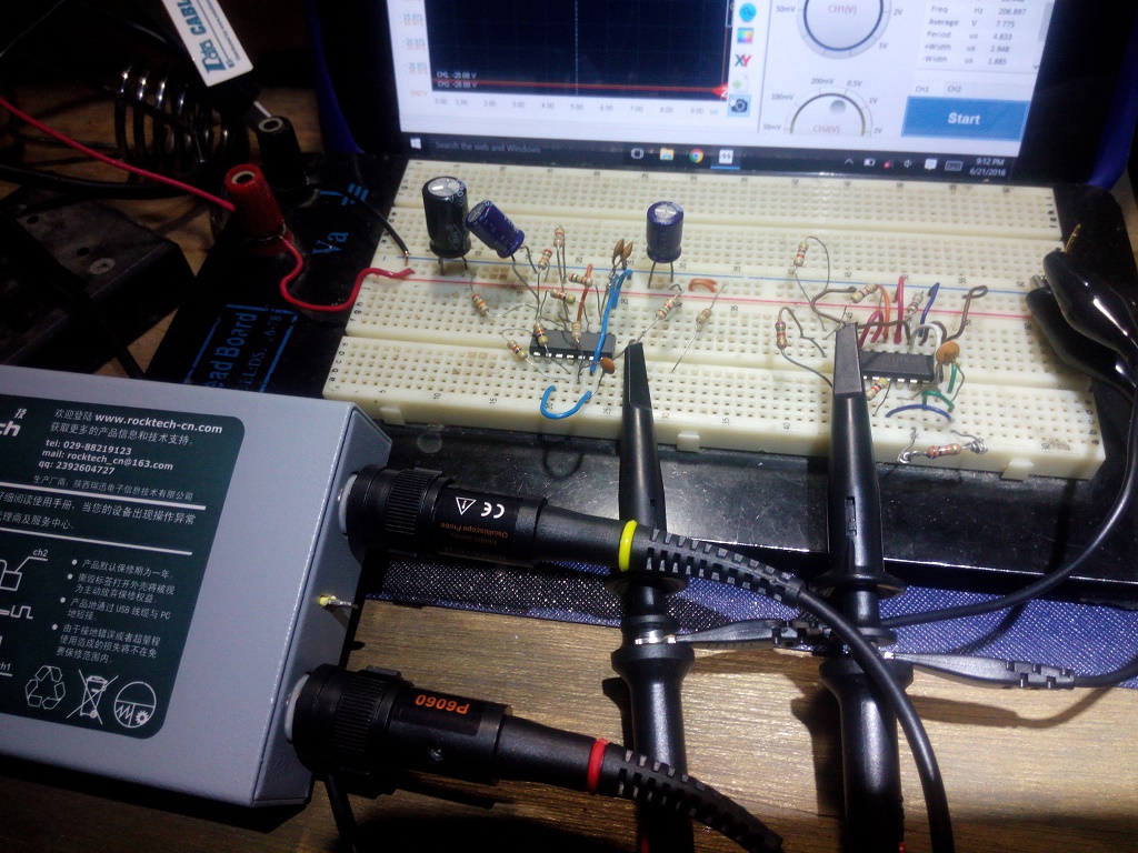

The blue trace is Tl494 while the yellow trace is Lm319
There is no speed difference between the two chips in terms of T rise and T fall therefore lm319 is as reliable as Tl494 in PWM audio generator. But when I try to increase the carrier signal from 235khz to 440khz Lm319 can still deliver respectable waveforms in fact I crank it up to 955khz and still produced good but slightly rounded corner pulses.
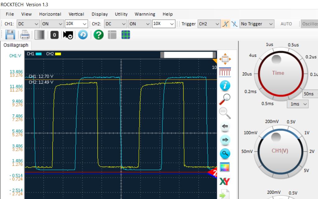
Real world probing of voltages across C2 in yellow trace, and across C4 in blue.
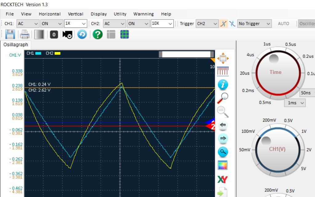

The image above was taken by probing the voltage across C4. Even a well trained eye may thought this is generated by a costly precision high speed comparator. It looks very linear to me.
In this breadboard scenario, output pin 12 of U2 produce ~11.2 volts peak at 51% duty factor (235khz) as seen from my digital scope. Then filtered by 25k resistor R10 and 10uf capacitor C5 to smooth it out into vicinity of ~5.6VDC. Another 25k resistor R5 were added so that the audio frequency and carrier frequency will not interact to each other. This is due to capacitor C5 that has a capacitive reactance of equal to short circuit to these two signals.
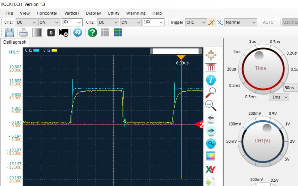
The blue trace is the input at pin 9 of U1 then the yellow trace is the output at pin 7.
I will add tuning mechanism at the output of U2 inserted between R3 and R7 because this is the culprit in making the duty factor to ~51%. R7 effectively add resistance to R3 during charging of C2 but discharges quicker via output transistor without R7 ugh!
Fig. 2. Circuit showing LM319 with duty factor correction using trimpot
Comparison output of U2 and U1. Blue trace is U2, Yellow trace is U1 at 51% on both.
This is the breadboard layout showing the added TC4420 FET driver. This is a preliminary sound testing that I need to check the quality of the sound it produce before I transfer the complete circuit into a PCB. This FET driver is qualified to drive my stock 5 watts speakers. I`m excited!

Note! There is no LC filter yet.
Here is the result output combined when amplified with FET driver. The blue trace is TC4420 and the yellow trace is LM319 at pin 7 of U1. The input buffer of TC4420 gives a sharp dual threshold voltage that improves the T rise and T fall of LM319. This is always needed to improve the switching efficiency of power FETs.
Very nice output improvement indeed.The blue trace is TC4420 and the yellow is LM319. The spikes at the trailing edge of the blue trace is just the capacitance of the test probe– nothing to worry.
When all the needed parts were in placed on the breadboard and test fire this thingy, – Lo and behold! the sound is surprisingly good!
What is my final say?
I can therefore say that generating triangular wave out of a simple resistor–capacitor network can give decent sound quality but at very low cost resulting to an effective design approach that can be reckoned with. Well, at least this is only if you dont want to buy precision high speed comparator online or just simply avoiding to spend much money for your next outdoor audio amp project. LM319 is as abundant as 555 timer IC, so you may add it into your arsenal of chips inline with your tl494 class d amp. If you appreciate the sound of TL494 as class D amp then you will like lm319 aslo.
But wait! the circuit drawing in Fig. 1 and 2 is the same circuit lay-out I made on my breadboard. this means you can expect some ringings on it from your scope due to long jumping wires and resistors leads that will radiate a lot. That lay-out you see on picture is the lowest possible noise I could do but trasfering to good PCB lay-out will give more satisfying sound performance.
Here is the sound that I apploaded in youtube using the built-in mic of my crappy smartphone. https://www.youtube.com/watch?v=fDZIXCRCzvI